EDA (Electronic Design Automation) Explained
- EDS Technologies
- September 18, 2024
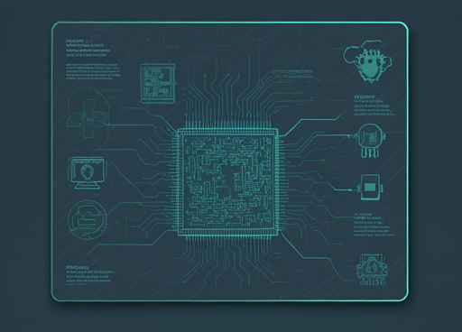
Electronic Design Automation (EDA) is a market segment encompassing software, hardware, and services aimed at defining, planning, designing, implementing, verifying, and manufacturing semiconductor devices, or chips. The manufacturing of these devices is primarily handled by semiconductor foundries, or fabs, which are highly complex and costly facilities. These fabs are either owned and operated by large, vertically integrated semiconductor companies or function as independent “pure-play” manufacturing service providers, the latter of which has become the dominant business model.

Recent Posts
-

From Prototypes to Production: How Additive Manufacturing is Shaping Atmanirbhar Bharat
The conversation around additive manufacturing (AM) in India has evolved considerably over the past decade. What was once viewed primarily as a prototyping technology is…
-

Identify Stray Light in Imaging Systems with LightTools
Stray light is undesired light radiation that interacts with the components of a system and degrades its performance by generating noise, that significantly reduces image…
-

Redefining the Riding Experience with RAMSIS
In two‑wheeler design, comfort and safety start with the rider. RAMSIS (Realistic Anthropometric Mathematical System of Interior Comfort Simulation) is an ergonomic simulation platform that…
-

Enhancing Product Understanding through 3D Technical Illustrator
The 3D Technical Illustrator role within the 3DEXPERIENCE Platform enables organizations to transform complex engineering data into clear, interactive, and visually rich technical documentation. In…
-

Transforming Physical Parts into Digital Models with CATIA 3DEXPERIENCE Reverse Engineer role
Reverse engineering has become a critical capability in modern product development, especially when working with legacy components, competitor benchmarking, or physical prototypes that lack digital…
-

Fixing Search Service Down Issue in 3DEXPERIENCE Platform
Search is one of the most critical features in the 3DEXPERIENCE platform. If the search service goes down, users cannot find objects, documents, or data—impacting…
-

Common Installation Errors and How to Fix Them in 3DEXPERIENCE
The 3DEXPERIENCE Platform is a powerful solution used by industries worldwide for product lifecycle management (PLM), simulation, and collaboration. However, installing 3DEXPERIENCE—especially on-premise—can be complex…
-

From Classroom to Industry: Empowering Future Engineers with the 3DEXPERIENCE Platform
In today’s fast-evolving engineering and design landscape, educational institutions must go beyond conventional CAD teaching methods. While standalone tools like CATIA V5, SOLIDWORKS, or traditional…
- EDS Technologies
- September 18, 2024
EDA (Electronic Design Automation) Explained
Electronic Design Automation (EDA) is a market segment encompassing software, hardware, and services aimed at defining, planning, designing, implementing, verifying, and manufacturing semiconductor devices, or chips. The manufacturing of these devices is primarily handled by semiconductor foundries, or fabs, which are highly complex and costly facilities. These fabs are either owned and operated by large, vertically integrated semiconductor companies or function as independent “pure-play” manufacturing service providers, the latter of which has become the dominant business model.