EDA (Electronic Design Automation) Explained
- admin_eds
- September 18, 2024
Electronic Design Automation (EDA) is a market segment encompassing software, hardware, and services aimed at defining, planning, designing, implementing, verifying, and manufacturing semiconductor devices, or chips. The manufacturing of these devices is primarily handled by semiconductor foundries, or fabs, which are highly complex and costly facilities. These fabs are either owned and operated by large, vertically integrated semiconductor companies or function as independent “pure-play” manufacturing service providers, the latter of which has become the dominant business model.

Recent Posts
-

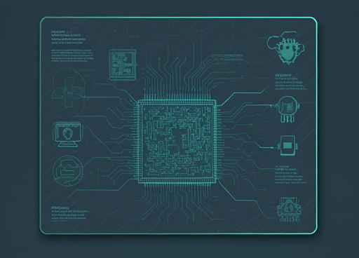
Enhancing Semiconductor Design with EDA Tools and Solutions
Overview; The semiconductor industry demands cutting-edge tools to address the complexities of modern chip design. As a trusted partner, EDS Technologies supports the adoption of…
-

Game Changing EOS Systems for Lifestyle and Consumer Goods Industry: Eyewear Applications
Every person’s face is as unique as their personality, making custom eyewear not just a luxury but a necessity for optimal comfort and functionality. Traditional…
-

Reinventing the Automotive Supply Chain with the Digital Experience Platform
Increased product complexity, global sourcing & disruptions, uncertainty, sustainability and regulatory pressures, consumer demand shifts, and cost pressures are some of the significant challenges that…
-

Transforming Prosthetics and Orthoses Manufacturing with the EOS SLS Process
The fields of prosthetics and orthoses have witnessed significant advancements in recent years, driven by the adoption of additive manufacturing (AM) technologies. Among these, the…
-

Accelerate the Development and Certification of Smarter Drones
The drone industry is rapidly evolving, offering solutions across numerous sectors like logistics, agriculture, surveillance, and environmental monitoring. With advancements in technology, drones are becoming…
-
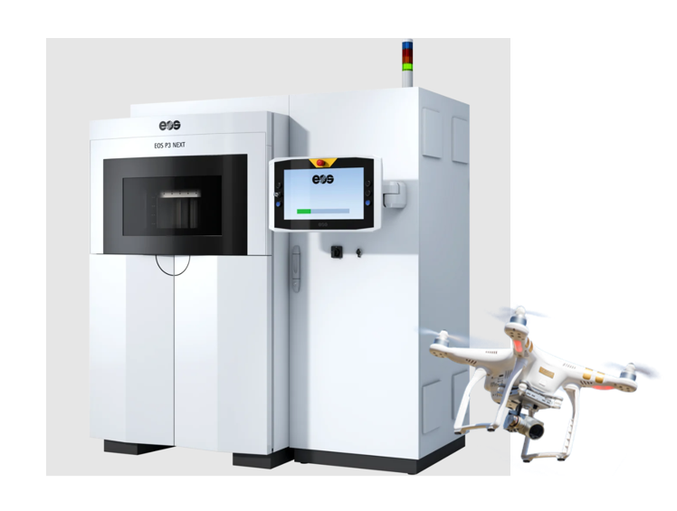
Drone Part Manufacturing: Leveraging DfAM and the EOS SLS Process
The rise of drones has revolutionized industries ranging from logistics and agriculture to filmmaking and defence. With their increasing adoption, the demand for lightweight, durable,…
-

Leveraging SIMULIA for Medical Device Innovation
The medical device industry requires innovation, precision, and compliance to deliver safe, effective, and reliable products. SIMULIA, as part of Dassault Systèmes' 3DEXPERIENCE platform, enables…
-

FEA Simulation of Medical Devices Using SIMULIA
The development of medical devices has seen significant advancements over the years, driven by innovations in technology, materials, and regulatory requirements. A crucial component in…
- admin_eds
- September 18, 2024
EDA (Electronic Design Automation) Explained
Electronic Design Automation (EDA) is a market segment encompassing software, hardware, and services aimed at defining, planning, designing, implementing, verifying, and manufacturing semiconductor devices, or chips. The manufacturing of these devices is primarily handled by semiconductor foundries, or fabs, which are highly complex and costly facilities. These fabs are either owned and operated by large, vertically integrated semiconductor companies or function as independent “pure-play” manufacturing service providers, the latter of which has become the dominant business model.